- HOME
- Advanced IC Substrate
IC Package
Substrate
Manufacturing Process
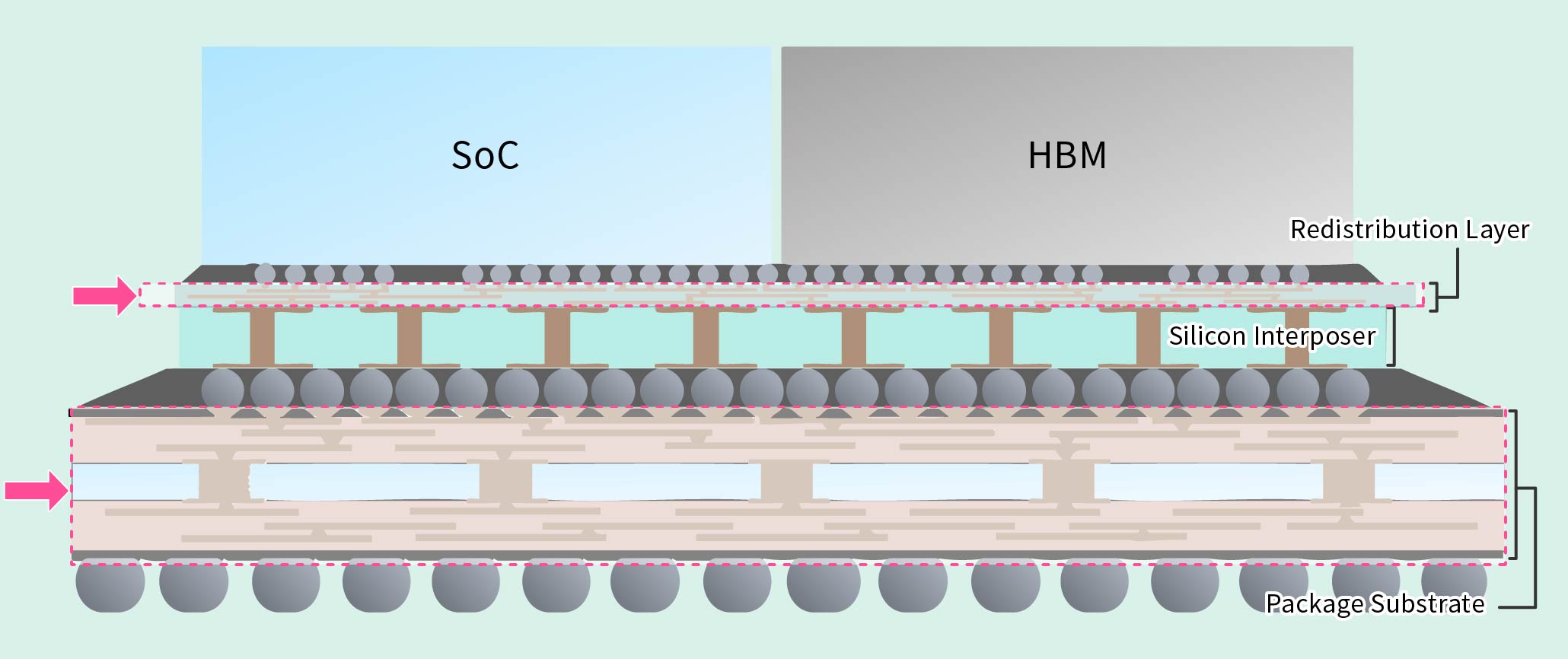
“Chiplet” technology attracts attention to support enhancement of high functionality in IC package and cost reduction. Silicon interposer is commonly used for inter-connection of chiplets in advanced IC package, while facing issues such as enlargement of package size, lower yield, higher cost.
Shin-Etsu Chemical developed excimer laser equipment to pattern embedded fine trace and small via by ablating insulation layer. The technology can be applied for package substrate, redistribution layer (RDL), organic interposer to replace silicon interposer function and conventional SAP process.
Process movie of advanced IC package substrate
Shin-Etsu Dual Damascene Process Features
By using Shin-Etsu excimer laser equipment, semiconductor front-end process technologies (Dual Damascene) can be applied to back-end process such as package substrate, redistribution layer (RDL), organic interposer substrate. (Shin-Etsu Dual Damascene Process)
Embedded trace process to replace SAP (Semi-Additive Process)
-
Shin-Etsu Dual Damascene Process
Process steps can be simplified, by excimer laser ablation to pattern insulation layer directly, rather than using DFR (Dry Film Resist), stepper and laser drill.
Unlike laser drill, the scanning process is not affected by number of vias per panel (good processability). Besides, it can process high-tapered vias. (to replace laser drill).
-
Issues of “SAP + laser drill”
DFR lamination, exposure and development process are required. As laser drill process is one by one process, the processing time is affected by number of vias while required number of vias are increasing recently.
Fine and high precision processing
Shin-Etsu original optical system enables fine and high precision processing.
-
Shin-Etsu Dual Damascene Process
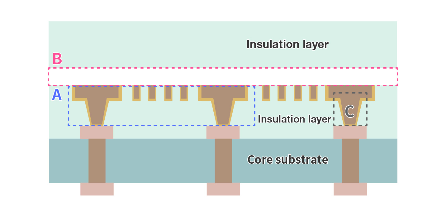
A【High alignment accuracy】
Shin-Etsu excimer laser equipment can achieve high alignment accuracy of processing both vias and traces.B【Embedded trace】
When laminating another layer, embedded trace reduce the risk of trace damage and electrical shortage.C【High taper】
Highly tapered small via and fine trace can be achieved by combination of Shin-Etsu optical system and excimer laser. -
Issues of “SAP + laser drill”
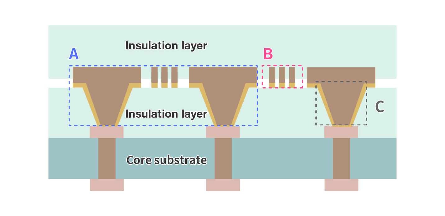
A【Alignment】
Limited alignment accuracy of laser drill, and need to align stepper and laser drill.B【Yield】
Trace damage risk when lamination, trace delamination risk, electrical shortage risk due to non-filling insulation material between traces.C【Limited precision of via】
Lower taper, not good at small via processing, low accuracy by laser drill.
Other benefits and applications
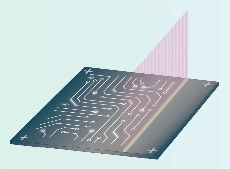
Not only IC substrate, Shin-Etsu excimer laser equipment can be used for various organic insulation materials such as RDL, organic interposer, and so on.
- Contribute reduction of build-up-layers by processing finer trace and smaller via.
- Contribute reduction of factory footprint by good throughput of excimer laser equipment instead of installing multiple laser drills.
- Improve electrical property and reliability of IC substrate and RDL due to embedded trace.