- HOME
- Micro Device
Micro Device Ultra-High-Speed Mounting Process
Devices are dramatically getting smaller and thinner. Besides, number of chips in electrical devices is remarkably increasing recently.
Shin-Etsu Chemical developed two types of high-speed mounting process by utilizing unique micro LED mounting technology.
-
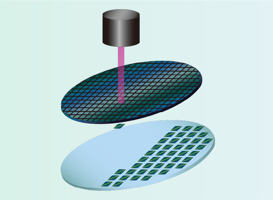
1) Laser mass transfer
①Mass transfer to Donor plate (Carrier)
②Mass transfer to substrate -
2) Stamp mass transfer
Mass transfer micro devices (①) to substrate
(Note: Shin-Etsu Chemical supplies stamp only, no supply of mounter/bonder)
Movie of high-speed micro device mounting
Shin-Etsu Laser Mass Transfer Technology(Shin-Etsu LMAT)
Laser mass transfer
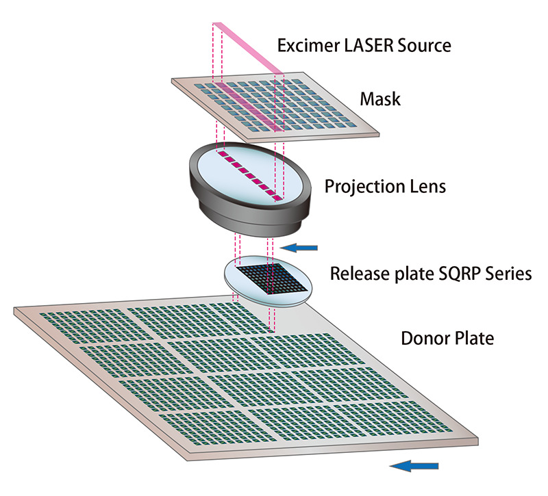
Number of devices in electrical equipment and package substrate is increasing year by year. And devices are getting thinner and smaller, therefore are hard to pick up by vacuum nozzle and are easily damaged by pick-up pin.
New solution is required by market, in consideration that increasing number of flip chip bonders is required (one by one pick-up and place takes longer tact time) which leads to more investment cost, larger footprint and more labor cost. Shin-Etsu Chemical offers high speed and high precision mounting process (dozens to thousands of devices per second).
Shin-Etsu Stamp Mass Transfer Technology(Shin-Etsu SMAT)
Stamp mass transfer
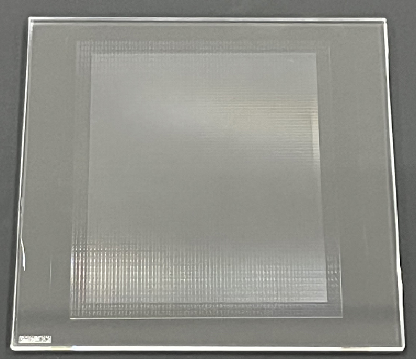
By utilizing their own unique material and molding technology, Shin-Etsu Chemical developed dot stamp (EZ-PETAMP) which has unique dot structure like Mt. Fuji, and whose fine-processed dot has good adhesion.
In combination with laser mass transfer technology, dozens to thousands of devices can be transferred per second with high-speed and high accuracy.
We can provide stamp bonder/mounter equipment suppliers with our stamp. (We don’t provide bonder/mounter)
